Lithography is a technique used to create integrated circuits by depositing thin layers of different materials on a silicon wafer. These materials are carefully chosen based on their electrical qualities and include semiconductors like silicon, germanium, and gallium arsenide. Wafer preparation, layer deposition, circuit design, and testing are only a few of the manufacturing process phases.
Integrated circuits, called ICs, are the building blocks of modern electronics, powering everything from cellphones to computers to satellites.
But how are these small electronics manufactured?
What materials and procedures are used to create these difficult silicon structures? In this blog, we will learn about and explore the fundamentals of how integrated circuits are manufactured, from the semiconductor materials utilised to the numerous fabrication techniques used.
Did you know?
India has a growing semiconductor industry and is currently home to several semiconductor manufacturing companies, including Intel, Samsung, and Texas Instruments.

History of the Integrated Circuit
- In 1947, William B. Shockley and his colleagues invented a small transistor that paved the way for the modern-day complex silicon fabrication used in integrated circuits. They discovered that adjusting an electron barrier on the surface of a crystal could control the flow of electricity through it, leading to the creation of small electronic devices.
- In 1958, Jack Kilby of Texas Instruments and Robert Noyce of Intel independently discovered a way to combine all components and their interconnections on a single silicon chip, creating the first integrated circuit. Kilby used germanium as a semiconductor material, while Noyce used silicon.
- Integrated circuits are categorised into analog, digital, and mixed based on their architecture and purpose. Analog ICs process continuous signals, digital ICs process discrete signals, and mixed ICs combine analog and digital functions on the same chip, making them suitable for various applications such as amplifiers, filters, microprocessors, or sensors.

Semiconductor Materials
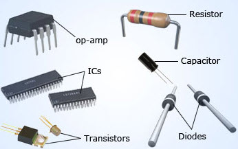
Transistors, diodes, and other components used in integrated circuits are made from semiconductor materials. These substances exhibit electrical characteristics that fall between conductors and insulators.
Under some circumstances, they can behave as insulators and under others, they can conduct electricity.
Types of Semiconductor Materials
In integrated circuits, a variety of semiconductor materials are employed, including:
1. Silicon
The most typical semiconductor material utilised in creating integrated circuits is silicon. This is due to silicon's superior electrical characteristics, abundance, and affordability. Additionally, it is readily available and straightforward to process.
2. Germanium
The first material utilised to make transistors was germanium. However, due to its low thermal stability and scarcity, silicon has mainly supplanted it. Infrared detectors are one area where germanium is still employed.
3. Gallium Arsenide
Applications that call for high-speed performance, including microwave communication systems, use gallium arsenide. It is more expensive than silicon yet has great electrical characteristics.
Also Read: Know Here How Your Favourite Hot Dogs Are Made [Ingredients and Procedure]
Characteristics of Semiconductor Materials
There are several characteristics of semiconductor materials; let’s have a look at some of them.
1. Conductivity
Doping is the addition of impurities to a semiconductor material to modify its electrical conductivity. N-type and P-type semiconductor materials can both be produced through doping.
Impurities like phosphorus or arsenic are introduced into the N-type semiconductor material. The material has excess free electrons, which are negatively charged because these impurities have one more electron than the silicon atom.
Impurities like boron or aluminium are introduced into a P-type semiconductor material. The substance lacks electrons, which are positively charged since these impurities have one fewer electron than the silicon atom.
2. Bandgap
The energy difference between a semiconductor material's valence and conduction bands is known as the bandgap. The conduction band is the region where electrons are free to flow, while the valence band is the region where electrons are strongly linked to atoms.
A semiconductor material's bandgap dictates whether it is an insulator or a conductor. In conductors, the valence band and conduction band overlap, enabling the unrestricted movement of electrons. The bandgap is too wide in insulators, preventing electrons from transitioning from the valence band to the conduction band.
Due to the tiny bandgap of semiconductor materials, doping levels can cause them to act like conductors or insulators.
3. Doping
Doping involves adding impurities to semiconductor materials to modify their electrical characteristics. N-type and P-type doping are the two most prevalent types of doping.
An impurity, such as phosphorus or arsenic, is added to the semiconductor material during N-type doping. Compared to the silicon atom, these impurities have one additional electron, resulting in an excess of free electrons, which are negatively charged.
An impurity, such as boron or aluminium, is added to the semiconductor substance during P-type doping. These impurities cause a shortage of electrons, which are positively charged because they have one fewer electron than the silicon atom.
How Are Integrated Circuits Made?
Integrated circuits are made through a complex and precise process of creating electronic components and their interconnections on a thin silicon substrate. Here are a few steps involved in developing an IC:
1. Wafer Preparation
Wafer preparation is the first step in IC fabrication. It involves cutting, shaping and polishing a thin slice of single-crystal silicon called a wafer. The silicon crystals used for wafer manufacturing are highly pure and grown from a silicon melt in a cylindrical shape called a boule.
2. Oxidation
The oxidation process can be described as a process designed to give oxygen to the silicon wafer to generate a layer of silicon oxide on the surface of the ICs. The process may take place in furnaces at very high temperatures.
The oxidation might be wet or dry depending on whether water vapour or oxygen gas is utilised as an oxidising agent. Wet oxidation is faster, while dry oxidation has better electrical properties. The SiO2 layer acts as an insulator and a mask for further processing steps.
3. Diffusion
Diffusion is the process of introducing impurities into selected areas of the silicon wafer to change its electrical characteristics. The impurities are called dopants and can be either n-type or p-type, depending on whether they donate or accept electrons into the silicon lattice.
The diffusion is done by heating the wafer in a furnace with a source of dopant gas, such as phosphine (PH3) for n-type or boron trifluoride (BF3) for p-type. The dopant atoms diffuse into silicon through openings in the SiO2 layer created by photolithography.
4. Ion Implantation
Ion implantation is an alternative method of doping the silicon wafer by bombarding it with a beam of high-energy ions of the desired dopant element. The ions penetrate into the silicon and create regions of n-type or p-type material.
Ion implantation controls dopant concentration and distribution more precisely than diffusion. Still, it also causes more damage to the silicon crystal structure that needs to be repaired by annealing.
5. Chemical Vapour Deposition (CVD)
The method of forming thin films of various materials on a silicon wafer by exposing it to a gas containing the desired element or compound is known as chemical vapour deposition (CVD).
The gas reacts with or decomposes on the wafer's surface, generating a solid coating. CVD can deposit materials including polysilicon, silicon nitride (Si3N4), metal silicides (like tungsten silicide WSi2), and metals (like aluminium Al).
6. Photolithography
Photolithography is the process of transferring a pattern from a mask to the surface of a wafer using light-sensitive materials called photoresists. The photoresist is coated on the wafer and then exposed to ultraviolet light through a mask that contains the desired pattern.
The mask can be positive or negative, depending on whether it blocks or passes light through its openings. The exposed areas of the photoresist become either soluble or insoluble in a developer solution, depending on whether it is a positive or negative photoresist.
The developed photoresist forms a patterned layer that can be used for further processing steps such as etching, doping or metallisation.
7. Metallisation
Metallisation is the process of forming metal interconnections between different regions or layers of an integrated circuit. The metal is usually aluminium or copper and is deposited on the surface by CVD or evaporation techniques.
The metal layer is then patterned by photolithography and etching to create wires and contacts that connect different components and terminals of the IC.
8. Packaging
It involves enclosing the finished IC chip in a protective casing that provides mechanical support, electrical connections and environmental protection. The packaging can be either plastic or ceramic and have different shapes and sizes depending on the application and performance requirements of the IC.
The packaging also contains pins or leads that connect the IC chip to external circuits or devices.
Also Read: What is the Process of Juice Manufacturing [Packaging and Processing Explained]
Challenges Facing the IC Industry
The IC industry faces several challenges affecting its innovation, growth and profitability. Some of these challenges are:
1. Innovation
The IC industry has followed Moore’s law for decades, which states that the number of transistors on a chip doubles every two years. However, as the feature size of ICs approaches the physical limits of silicon technology, the IC industry faces increasing challenges in maintaining the pace of scaling while ensuring performance, reliability and cost-effectiveness.
These challenges include power consumption, heat dissipation, variability, leakage, noise and defects. Thus, the innovation of ICs is important in pushing innovation in electronic devices and modern-day internet infrastructure.
2. Robotics and Artificial Intelligence
The IC industry increasingly uses robotics and artificial intelligence (AI) to automate and optimise its manufacturing processes, such as wafer handling, testing, inspection and quality control. Robotics and AI can improve IC fabrication productivity, accuracy, reliability and safety. However, they also pose challenges such as high costs, technical complexity, and cybersecurity risks.
3. Geopolitical Tension and Trade Dispute
The geopolitical tension and trade conflict between significant players in the IC business, such as the United States and China, is a third challenge. The US has imposed penalties and restrictions on Chinese businesses such as Huawei and SMIC, which rely on US technology and equipment for IC fabrication.
China has responded by investing heavily in its domestic IC industry and seeking alternative suppliers. The conflict has created uncertainty and instability in the global IC market and may affect collaboration and innovation within the industry.
Conclusion
Integrated circuits (ICs) are the fundamental components of modern electronics and modern-day devices. Everything ranging from smartphones to tiny cameras contains a silicon chip for complex integrated circuits.
Deposition, photoresist, lithography, etch, ionisation, and packaging are complicated and precise procedures used to manufacture integrated circuits. Integrated circuits are critical to the growth of the modern-day economy and the development of a wide technological infrastructure such as AI, large data warehouses, etc.
Follow Khatabook for the latest updates, news blogs, and articles related to micro, small and medium enterprises (MSMEs), business tips, income tax, GST, salary, and accounting.
